In situ SEM Stages
Control and sense technology.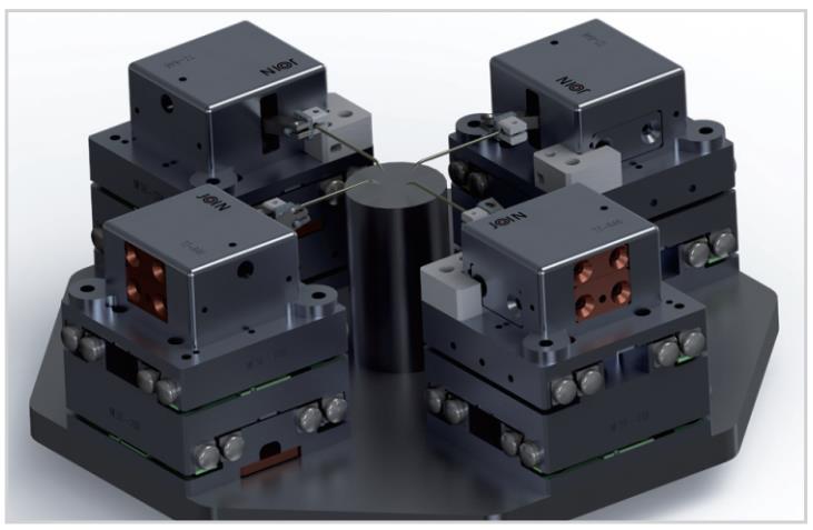
Nanoprobe for SEM/FIB
Compatible to any SEM and FIB. Probe controlled by 3D nanopositioner. Up to 8 probes could be installed on one sample stage. The probe have sub nanometer resolution with minimeter movement range. The probe could be replaced by fiber probe, force sensor, tweezer.
Specification
- - Movement range: XYZ ±10mm;
- - Movement resolution: XYZ 0.5nm;
- - Maxmium velocity: 3mm/s;
- - Controlled by manual pad or software.
Application example
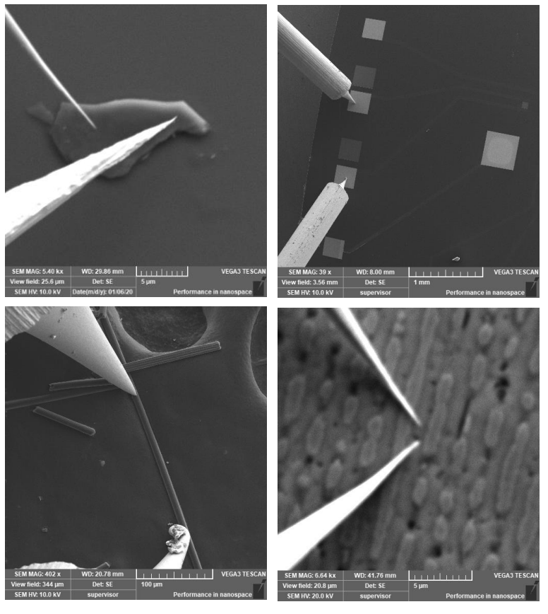
Top left: measure 2D materials. Top gight: measure a device. Bottom left: measure 1D materials. Bottom right: measure a chip.
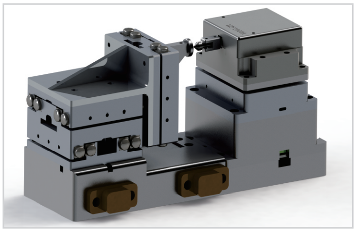
Nanoindentor for SEM
Nanoindentor for SEM could quantitatively analysis the mechanical property at micro scale. At the same time, SEM image the process lively.
Nanoindentor specification
- - Mode: indentor, push, pull;
- - Maxmium load: 100mN;
- - Indentor close loop movement range: 100um;
- - Indentor close loop movement resolution: 2nm.
- - Sample side movement range: ±10mm, 3 axis or 4 axis;
- - Sample side movement range: ±10mm;
- - Sample and tip can be heat up to 600℃;
- - Easy exchange indentor tip.
Application example
Tense a micro ball.
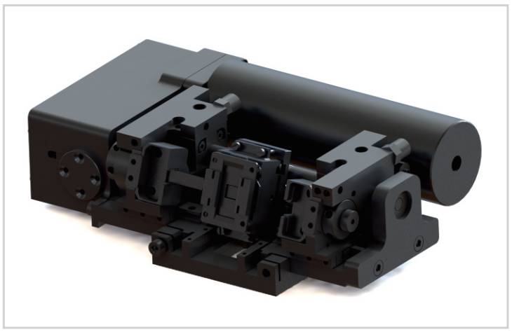
SEM tensile stage
Tensile stage for bulk sample.Up to 5000N 800℃. Compatible to EBSD.
Specification
- - Mode: tense, comprise, bend;
- - Load capacity: 1000,2000, 5000N;
- - Movement range: 30mm;
- - Mvement resolution: 20nm.
- - Velocity: 0.1~50um/s;
- - Heating stage: 600℃/800℃
- - Compatible to EBSD.
Application example
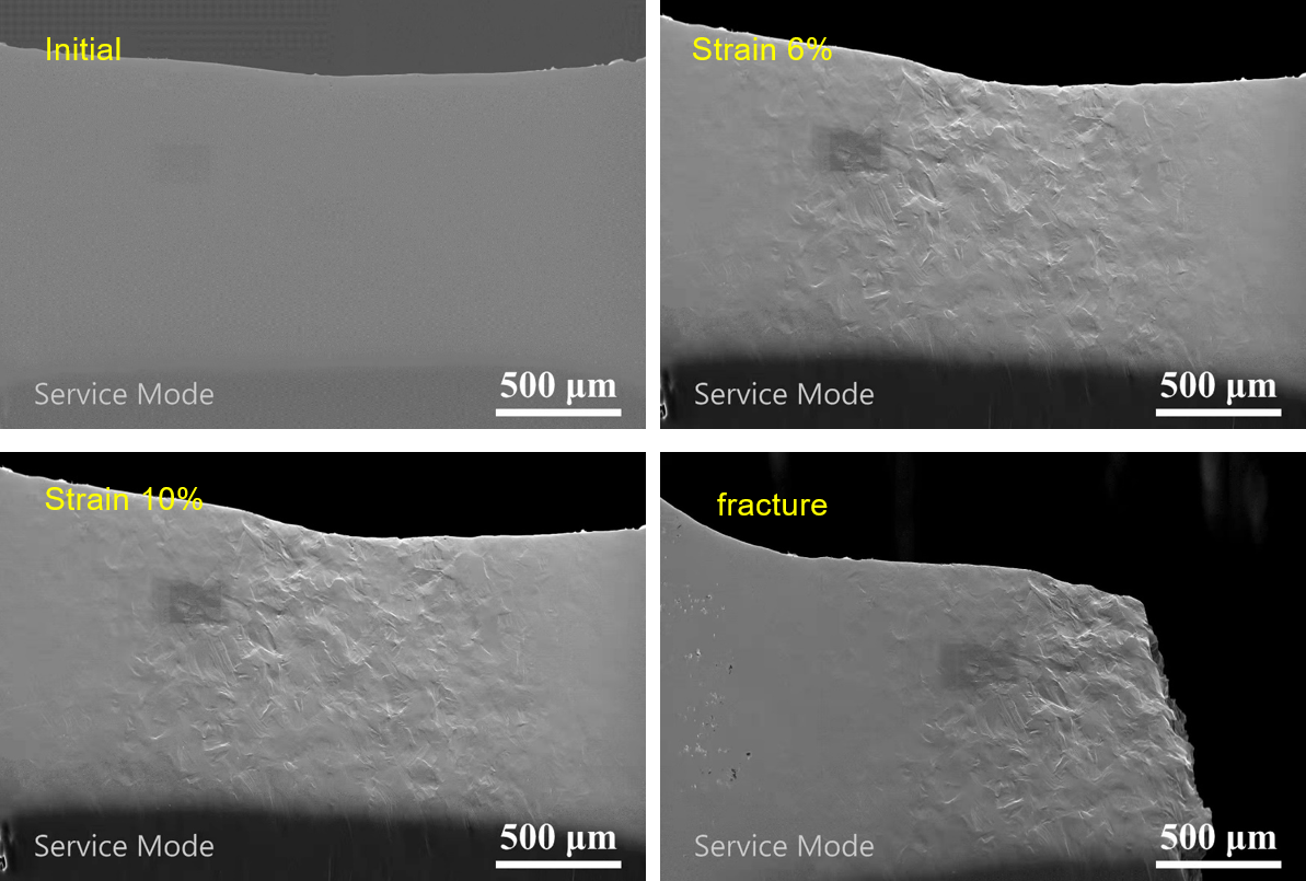
Tense a metal sample
EBSD analysis at different strain.
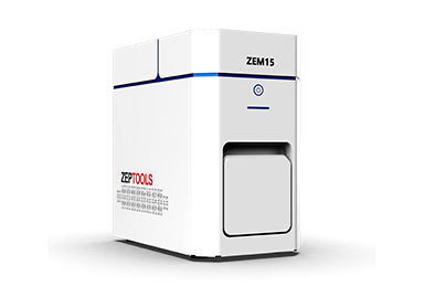
Desktop SEM-ZEM15
ZEM15 is a desktop SEM released by ZEPTOOLS in 2019. Its acceleration voltage is 15KV. Both secondary electron detector and back scatter electron detector are equiped. EDS is an option. Resolution of ZEM15 could be better than 6nm.